
Abstract
Catalytic formation of nanochannels in the surface layers of both pure diamond crystallites and conductive boron-doped diamond (BDD) electrodes was performed using a few metal nanoparticles (Co, Nb, Mo, and W) in a hydrogen atmosphere. Thermogravimetry in the hydrogen atmosphere showed the beginning of the consumption of diamond at temperatures higher than ca.  . The nanochannels grew parallel to the crystallite edges, and had a characteristic morphology consisting of flat walls perpendicular to the flat base. The extent of the channeling behavior did not depend on the content of the boron in the BDD. Cyclic voltammetry showed that the surface area of the BDD was increased several times over by the formation of the nanochannels and holes. This simple method to increase the surface area of diamond materials is useful for introducing several new functionalities, including the production of high-current-density BDD electrodes, and of loading-sites for fine catalyst metals or compounds, etc.
Export citation and abstract BibTeX RIS
Although the nanoscale control of the shape of fullerenes,1 carbon nanotubes,2 and graphite3–9 has been widely investigated, the nanoscale morphological modification of the surface layers of diamond has not yet been established. Chemical etching of pure diamond with  or oxygen has been investigated;10 however, the chemical creation of nanopores or nanochannels on them has not yet been reported. The different available forms of diamond, such as crystallites, powders, and coatings, have been utilized for a variety of purposes, including in jewelry, polishing and grinding applications, and heat-radiation applications for large scale integration (LSI). In addition to pure diamond, conductive boron-doped diamond (BDD) electrodes grown by chemical vapor deposition on metal or silicon substrates11, 12 are useful due to their wide potential range and significant chemical stability when compared to graphite electrodes.13, 14 A number of potential applications of BDD have already been proposed, including electroanalysis,15 electrosyn thesis16 and the electrochemical treatment of wastewater.17, 18 When BDD is used for a large-scale electrolysis process,19, 20 the larger the surface area of the BDD, the higher will be the practical current density. However, it is difficult to change the surface of the BDD into a porous structure in order to increase the surface area. In an attempt to increase the surface area of the BDD, Fujishima and his co-workers succeeded in fabricating well ordered nanoporous honeycomb diamond films by oxygen plasma etching through an alumina mask on mirror-polished BDD.21–24 Although this method can create well ordered nanopores on the BDD, it cannot be applied from a practical point of view for the creation of nanopores in large-scale BDD electrodes. Therefore, a simple method that can form a large number of nanoholes or nanochannels in the surface layers of the BDDs needs to be developed.
We now report our discovery of the catalytic formation of nanochannels in the surface layers of synthetic pure diamond crystallites and BDDs using cobalt, molybdenum, niobium, and tungsten nanoparticles at  in a hydrogen atmosphere. As similar methods to this investigation, there was reported a catalytic etching technique using metals as a promising method for obtaining thin diamond films efficiently. In those papers, it was supposed that the diamond converts into graphite by the catalysis under the appropriate temperature
  condition, and then the converted graphite diffuses into the substrate.25–30 On the other hand, Ralchenko et al. dealt with diamond etching in a
  atmosphere through thin solid metal layer for the patterning of diamond surfaces.31
Experimental
A  aqueous solution of
  was used as the source of the cobalt nanoparticles. After
  of the precursor solution was dropped onto
  of a synthetic single-crystal diamond powder (Tomei Diamond Co., Ltd.; No. MD-200). This synthetic diamond was statically produced on an ultrahigh pressure (
 ,
,  ,
,  ) followed by crushing with iron balls, and then washed with acid and water to remove the iron. The powder was placed in a Pt boat which was then placed in a fused silica furnace tube, dried at
  in flowing
  gas, and then heated at
  in a flowing gas mixture of
  for
for  . The purity of both hydrogen and nitrogen used are guaranteed higher than 99.999%. The specimen treated by this procedure was designated as Co-treated diamond crystallites in this paper.
The BDD was purchased from Fraunhofer Institut Schicht-und Oberflächentechnik (boron concentration is  ). A
). A  aqueous solution of
  ,
,  ,
,  , or
, or  was used as the source of the metal nanoparticles. After
  of the precursor solution was dropped onto a small cut (ca.
  ) BDD specimen of ca.
  , the specimen was placed on a Pt boat, placed in a fused silica furnace tube, dried at
  in a flowing
  gas, and then heated at
  in a flowing gas mixture of
  for
for  . The specimen treated by this procedure was designated as
  ,
,  , Nb or W-treated BDD in this paper. The high-resolution scanning electron microscopy (HR-SEM) images were obtained using a Hitachi S-5000 scanning electron microscope.
Results and Discussion
Figures 1A and B show HR-SEM images of as-received synthetic diamond crystallites. Although some stripes, probably edges, are seen on the surface, neither holes nor channels can be observed. None of metallic particles are observed on the surface as shown in the backscattering electron image of the specimen, (Fig. 1B). Cobalt nanoparticles were loaded on the diamond crystallites by an impregnation method with  , and the specimen was heated under a gas mixture stream of high purity
  . Based on a thermogravimetry, the decomposition of
  loaded on the diamond particles was achieved at
  , and the consumption of the diamond began beyond ca.
  . The
. The  -loaded specimen was heated in the hydrogen atmosphere at
  for
for  , and its HR-SEM images are shown in Fig. 1C, where the left micrograph is a secondary electron image and the right one is a reflection electron image. As shown in Fig. 1C, channels are introduced in the surface layers of the diamond crystallites. Note that the bases of the channels are flat and the walls of the channels are perpendicular to the bases. The cobalt particles may have been in a melted state when the diamond surface layers were catalytically etched by the cobalt particles analogous to the case proposed by Baker for the grooving of graphite layers by nickel particles.6 The white spots ca.
  in diameter at the ends of the channels in the reflection image of Fig. 1C are cobalt particles. Due to the flatness of the crystallite surface, the cobalt particles on the diamond surface grew larger with the heat-treatment time under the hydrogen atmosphere due to the aggregation with each other in this case. Only methane was detected in the gaseous product by gas chromatography during the heating of the specimen above
  in the hydrogen atmosphere.
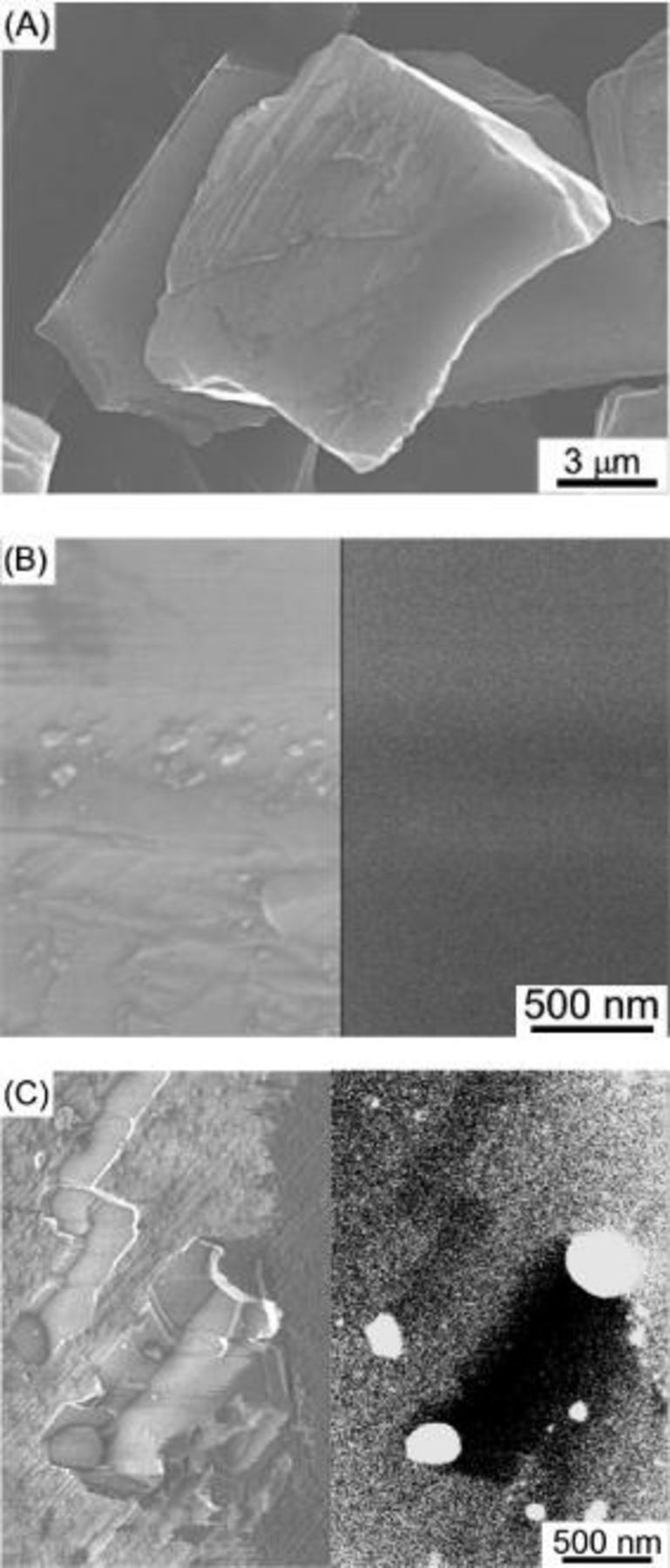
Figure 1. SEM images of the as-received and Co-treated diamond crystallites under a gas mixture stream of highly pure  at
at  for
for  . (A) The as-received diamond crystallites. (B) A secondary electron image (left) and its reflection image (right) of the diamond crystallite at high magnification. (C) A secondary electron image (left) and its backscattering electron image (right) of the Co-treated diamond crystallites. The white spots ca.
  in diameter in the reflection image of (C) are cobalt nanoparticles.
Figure 2A shows an HR-SEM of the surface of the as-received BDD which is composed of small crystallites with flat surfaces in a tight formation, which is the typical surface texture of the BDD with  ,
,  , and
, and  facets. By heat-treating the Co-loaded BDD in the hydrogen atmosphere at
  for
for  , a number of nanoholes and linear nanochannels were created, not only at the grain boundaries, but also on the terraces, as shown in Fig. 2B. At a higher magnification as shown in Fig. 2C, it can be clearly seen that the walls of the nanoholes are parallel to the edges of the diamond crystallite grains. Similar to the nanochannels formed in the surface layers of the pure diamond crystallites by the Co particles, the bases of the channels formed in the surface layers of the BDD are flat and the walls of the channels are perpendicular to the bases. No appreciable effect of the
  ligand on the morphology of the nanochannels was observed when we compared Fig. 2 with the HR-SEM images of the Co-treated specimen, in which the cobalt nanoparticles were deposited onto the BDD by vacuum evaporation.
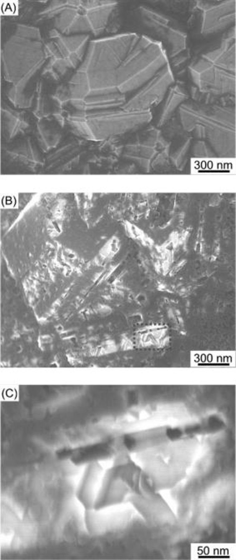
Figure 2. SEM images of the as-received and the Co-treated BDD under a gas mixture stream of highly pure  at
at  for
for  . (A) The as-received BDD. (B) The Co-treated BDD. (C) A high-magnification image of part of (B) shown by the rectangle.
As a metal with a higher melting point than cobalt  , molybdenum
  was used in an attempt to etch the BDD. Figure 3 shows the HR-SEM images of the Mo-treated BDD at
  in a flowing gas mixture of
  for
for  . Similar to the Co-treated BDD, many nanoholes and nanochannels are created, not only at the grain boundaries but also on the terraces. A backscattering electron image of the Mo-treated BDD surface shown in Fig. 4B demonstrates that the pores are created by the Mo nanoparticles, which are seen as white circles in the reflection image. Similar to the channels formed on the pure diamond crystallites and the BDD by cobalt nanoparticles, the bases of the channels are flat and the walls of the channel are perpendicular to the bases of the diamond as seen in Fig. 3C. As the melting point of molybdenum is very high,
  , the molybdenum particles might not be in a melted state even if the melting point of the metal generally decreases with a decrease in the metal particle size. Analogous to the Mo-treated BDD, straight nanochannels were formed in the surface layers of the Nb-treated and W-treated BDDs as shown in Fig. 4.
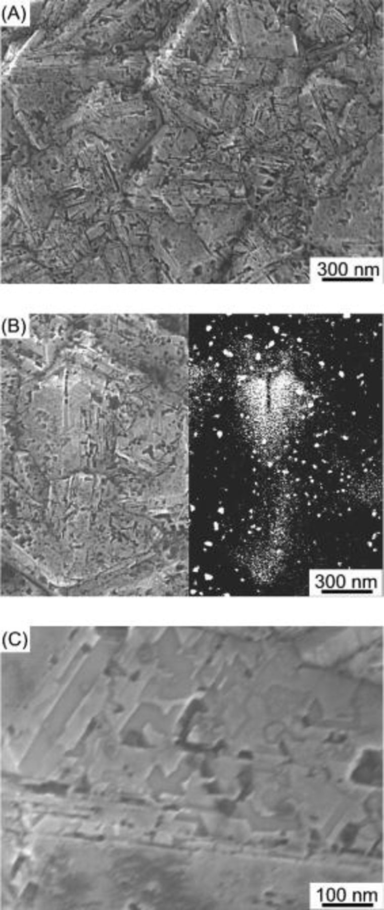
Figure 3. SEM images of the Mo-treated BDD under a gas mixture stream of highly pure  at
at  for
for  . (A) Outline. (B) Comparison of the secondary electron image (left) and the backscattering electron image (right). (C) A high-magnification image of part of (B).
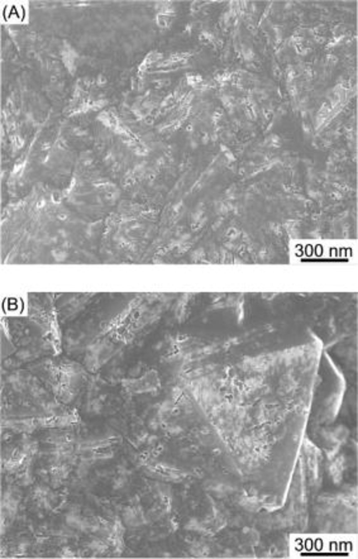
Figure 4. SEM images of the Nb-treated and W-treated BDDs under a gas mixture stream of highly pure  at
at  for
for  . (A) Nb-treated BDD. (B) W-treated BDD.
Although the reason for the channeling of diamonds by the metal nanoparticles and the consequent channels of a few tens or a few hundred surface layers remains unclear, one possibility is the formation of a carbide-like layer containing hydrogen at the interface of the metal nanoparticles with the diamonds prior to the formation of methane. Formation of graphite-like layer, instead of the carbide-like layer, might have been formed at the metal-diamond interface; however, formation of methane suggests the formation of the former species. The clarification of this argument is under investigation. Both the diamond surface and these metals have a strong affinity for hydrogen.10, 32–34 The successive formation of a carbide-like surface layer containing hydrogen could have assisted the moving of the metal nanoparticles, resulting in the channeling of the surface layer of the BDD. The fact that the bases of the nanochannels formed on the BDD are flat and the walls are perpendicular to the bases suggests that particular crystal planes are easy to be etched. The precise mechanism of the linear channeling of the metal nanoparticles along the specified directions of the diamonds by the metal nanoparticles and the effect of the particle size on the channeling phenomenon are currently under investigation.
Figure 5 shows the cyclic voltammograms (CVs) of the BDD and the Co-treated BDD electrodes in 
 at
at  . The cobalt nanoparticles remaining on the surface layers of the Co-treated BDD was removed with
 at
at  . The specific capacitance of the Co-treated BDD determined from the voltammogram between
  vs RHE was
  and that of the nontreated BDD was
  . This means that the electrochemical surface area of the BDD was increased several time over after the Co-treatment. The anodic current above
  vs RHE is the characteristic of the BDD, and the increase of it after the Co-treatment is due to the increase of the surface area. Little difference was observed on the Raman spectra of the BDD and the Co-treated BDD electrodes both having a very small amount of sp2 carbons. Thus, the Co-treatment of the BDD can increase its surface area with little change of the chemical properties of the BDD surface.
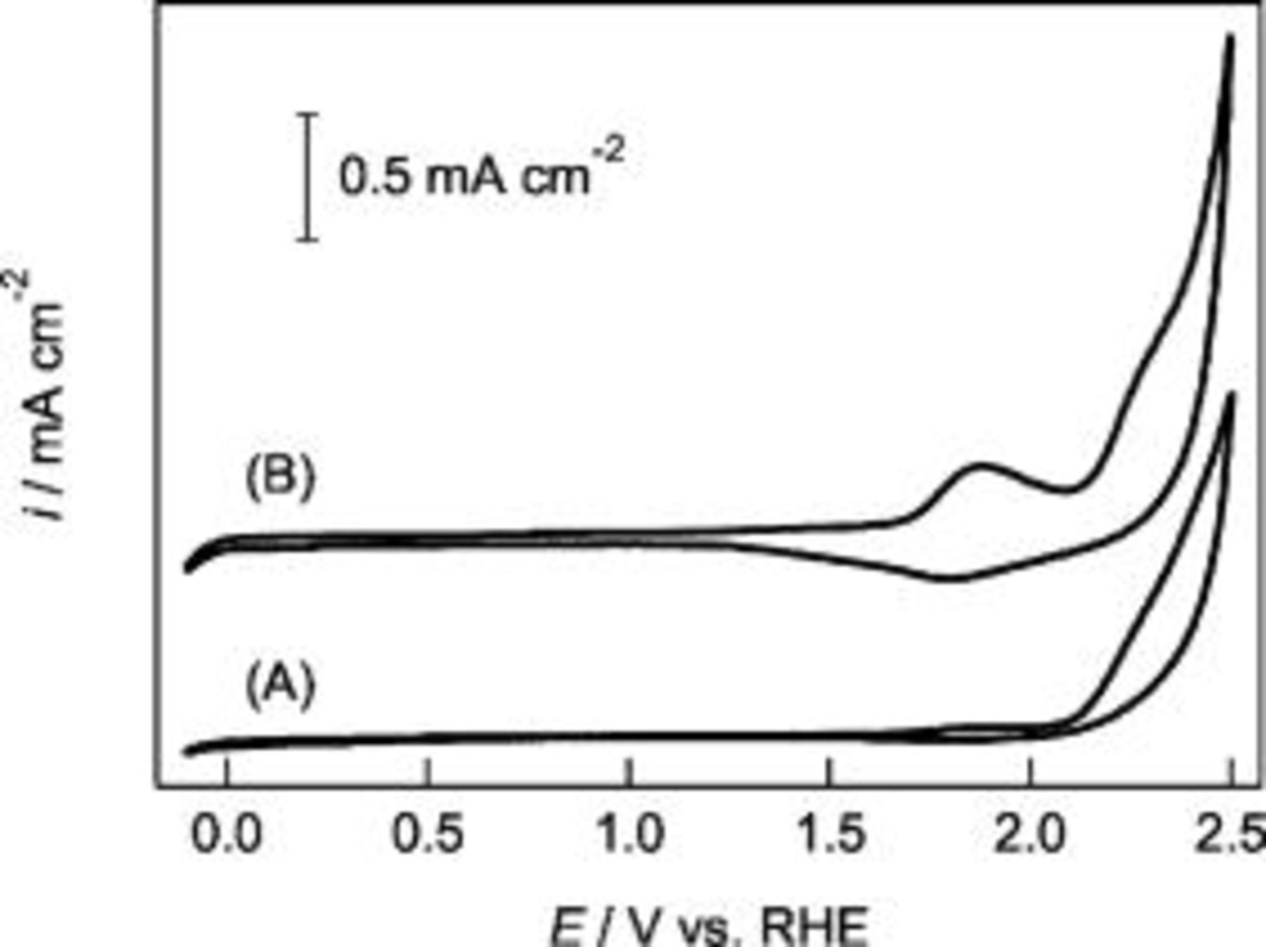
Figure 5. CVs of the as received BDD and the Co-treated BDD under a gas mixture stream of highly pure  at
at  for
for  . (A) BDD. (B) Co-treated BDD which was followed by removing of the Co particles with
 at
at  . These voltammograms were measured in
 at
at  with a potential sweep rate of
  .
.
Conclusions
We have discovered a unique etching phenomena using Co, Nb, Mo, and W nanoparticles of the pure diamond crystallites and the BDD electrode material under a hydrogen atmosphere at  . The shapes of the etch pits, i.e., nanochannels and nanoholes, were affected by the arrangement of the carbon atoms in the diamond crystals. This simple method can be used to increase the real surface area of the diamond, BDD electrodes, or other carbon materials. The nanochannels on BDD can also be utilized to form the sites for the implantation of any metal or compound particle catalysts. Although this method can be applied for the increase of the surface area of large-scale BDD electrodes, the method using ion-etching method21–23 must be difficult to be applied for large-scale BDD electrodes. The use of metal films or plates to etch diamonds is useful for the modification of the surface morphology of diamond and BDDs; however, both methods are difficult to form nanoscale channels and holes on the surface layers of diamonds.
Shinshu University assisted in meeting the publication costs of this article.