

Abstract
Photocatalytic water splitting is a promising method for hydrogen production, and the search for efficient photocatalysts has received extensive attention. Two-dimensional van der Waals (vdW) heterostructures have recently been considered excellent candidates for photocatalytic water splitting. In this work, a BP-MoSe2 vdW heterostructure composed of a blue phosphorus (BP) and MoSe2 monolayer was studied as a potential photocatalyst for water splitting using first-principles calculations. The results show that the heterostructure has a type-II band structure, and the band edges straddle water redox potentials under biaxial strains from −3% to 2%, satisfying the requirements for photocatalytic water splitting. In addition, the heterostructure has excellent power conversion efficiency (PCE) and strong optical absorption in both visible light and near-ultraviolet region, indicating that it is a very promising candidate for photocatalytic water splitting. Specifically, the PCE was enhanced to ∼20.2% under a tensile strain of 2%. The Gibbs free energy profiles indicate that BP-MoSe2 vdW heterostructure exhibits good catalytic performance in hydrogen and oxygen evolution reactions. In particular, high carrier mobility implies that the transfer of carriers to reactive sites is easy, and the recombination probability of photogenerated electron–hole pairs is reduced.
Export citation and abstract BibTeX RIS
1. Introduction
Hydrogen energy is a clean, environmental friendly, pollution-free, abound in natural resources and renewable new energy, and thus developing hydrogen energy is one of the effective ways to solve environmental pollution. So far, large-scale and low-cost hydrogen production is one of the most challenging technologies for hydrogen application and the first issue of hydrogen economy. Since Sunlight and water are the most abundant, clean and renewable natural sources on the Earth, photocatalytic water splitting is thus considered a sustainable way to make hydrogen [1]. However, the lack of efficient and inexpensive hydrogen production catalyst is the key to hamper the hydrogen development. Therefore, identifying the efficient photocatalyst is essential for water splitting to produce hydrogen.
Two dimensional (2D) materials have been considered as the best candidates for photocatalysts in water splitting due to the large surface-volume ratio and short migration distance to the reaction surface for photogenerated carriers [2], some 2D materials such as g-C3N4 [3] and MPS3 (M = Fe or Mn) [4, 5] have been proved good photocatalysts for water splitting in experiments. Recently, 2D van der Waals (vdW) heterostructure material as a new family of photocatalysts has been proposed for water splitting due to their unique structure, type-II energy band, moderate bandgap and suitable band edge position. For example, Kou et al recently reported a review of research progresses of 2D Janus vdW heterojunctions, which summarized the fundamental properties including electronic structure, interface contact and optical properties, and discussed the potential applications in photocatalytic water splitting and energy conversion devices [6]. In addition, ZnO-based vdW heterostructures such as ZnO/BSe [7], CdS/ZnO [8], and ZnO/GaN [9] have been investigated as promising photocatalysts for water splitting using the first-principles calculations. Moreover, C2N-based type-II heterostructures such as C2N/WS2 [10], C2N/GaTe and C2N/InTe [11] were predicted theoretically to be promising water splitting photocatalysts. In experiment, vertically stacked WS2/MoS2 bilayer heterostructures with type-II band alignment and the clean interface had been successfully fabricated at high temperature using epitaxial growth techniques [12], the MoS2/WSe2 type-II vdW heterojunction had been obtained by vertical stacking of 2D materials, which are held together by vdW forces and contain atomically sharp interfaces [13]. Furthermore, the vertical heterostructures formed by narrow-bandgap black phosphorus and large-bandgap MoS2 with tunable band-structure alignment had been fabricated experimentally [14]. More recently, layered transition metal dichalcogenides have been focused on and shown great potential in the field of photocatalysts for water splitting [15–19]. As the representative example, the single layer MoSe2 has good thermal stability with an optical direct bandgap of 1.55 eV, and thus it can be expected to apply in the relevant device involving the solar spectrum [20]. On the other hand, blue phosphorus (BP), a new 2D semiconductor material with a buckled graphene-like structure, has been successfully synthesized in the experiment after being proved to be thermostable theoretically [21–23]. Then, the BP has been widely investigated both experimentally and theoretically [24–28]. More specifically, BP-based vdW heterostructures have been extensively studied for its applications in photocatalytic water splitting [29–44]. For instance, BlueP/GeC and BlueP/SiC are predicated to be promising high performance photocatalysts for water splitting [37]. In addition, the bandgaps and carrier concentration of the BlueP/WSe2 vdW heterostructure can be modulated by the vertical compressive strain [38]. The power conversion efficiency (PCE) of the BlueP/MoSSe vdW heterostructure can be achieved 19.9% under a 2% tensile strain [41]. It worth noting that there is a strong electrostatic electric field at the interface of the BP-based heterostructures such as BP/g-GaN [29], BP/g-ZnO [33], BP/MoSSe [35], and BP/BSe [43], resulting in the photogenerated electrons transfer from the g-GaN, g-ZnO, MoSSe and BSe layer to the BP layer. Therefore the BP layer can acts as an electrons accepter while the counterpart acts as an electrons donor, giving rise to dual function of separating photoinduced charge carriers and extending their lifetimes.
Motivated by the above works, the BP-MoSe2 vdW heterostructure has been constructed in this work. The stability, electronic structures, biaxial strain effects, PCE and optical absorption, Gibbs free energy for hydrogen evolution reaction (HER) and oxygen evolution reaction (OER), as well as the carriers mobility of the BP-MoSe2 vdW heterostructure have been systematically studied using the first-principles calculations. Our results indicate that the BP-MoSe2 vdW heterostructure is robust stable and has many advantages for photocatalytic water splitting. More important, we unveil the origin of the excellent PCE of the BP-MoSe2 vdW heterostructure under biaxial tensile strains.
2. Computational details
All the first-principles calculations based on density functional theory in this work were performed using the Vienna Ab Initio Simulation Package [45, 46]. The interaction between electrons and ions was described by the projected augmented plane-wave (PAW) with the cutoff energy of 500 eV [47, 48], and the exchange and correlation functional of the GGA in the Perdew–Burke–Ernzerhof (PBE) form was used [49]. In addition, the gamma centered Monkhorst–Pack scheme [50] was to sample the Brillouin zone, and the Grimme's semi-empirical DFT-D3 method was considered to describe the long-range vdW interactions [51, 52]. Meanwhile, the atomic positions and lattice parameters were fully relaxed until the total energy is converged to 1.0 × 10⁻⁴ eV and the force on each atom is less than 0.02 eV Å−1. In order to avoid the interactions between the periodic images, a vacuum region of 25 Å in the z direction was added in the unit cells. The dipole correction was adopted in all calculations to eliminate the errors caused by periodic boundary conditions. Since the standard GGA functionals tend to underestimate the band gap of a semiconductor, thus a Heyd–Scuseria–Ernzerhof hybrid functional (HSE06) [53] was used to compute the electronic structures of the BP and MoSe2 monolayer and the BP-MoSe2 vdW heterostructure with the optimized geometries. The spin–orbit coupling (SOC) effects for the BP, MoSe2 monolayer and the BP-MoSe2 vdW heterostructure have also been examined in terms of the first variation method at the GGA-PBE level. To include strong correlation effects, GGA + U calculations were performed with an effective U value (Ueff = U−J) of 3.0 eV to modify the 3d orbital of Mo atom [54, 55]. In addition, in ab initio molecular dynamics (AIMD) simulations, the 5 × 5 supercell (125 atoms) for the BP-MoSe2 vdW heterostructure was used as the initial geometry with a 1 × 1 × 1 k-point mesh at the Γ-point. All the AIMD simulations were conducted with the NVT ensemble. A Verlet algorithm was integrated with Newton's equations of motion at a time step of 1 fs for a total simulation time of 10 ps.
3. Results and discussion
3.1. The geometry, stability and electronic structures of the BP-MoSe2 vdW heterostructure
First of all, the structural and electronic properties of the BP and MoSe2 monolayer have been optimized. Since monolayer MoSe2 shows large spin-splitting in both valence and conduction bands induced by SOC [56], we performed test calculations for the BP, MoSe2 monolayer and the BP-MoSe2 vdW heterostructure with and without SOC. As shown in figure 1(a), obviously, the SOC breaks the spin degeneracy of the valence and conduction bands in the MoSe2 monolayer. Furthermore, it is found that SOC induces spin splitting of 246.7 meV at the valence band maximum (VBM) and 14 meV at the conduct band minimum (CBM), which agrees well with the results in [56], where 188 meV at the VBM and 20 meV at the CBM. However, figure 1(b) shows that the SOC in the BP monolayer is weak enough to be ignored. This observation originates from the fact that the SOC is stronger for heavier atoms. More importantly, the positions of the VBM and CBM in the BP-MoSe2 vdW heterostructure with SOC are almost the same as those without SOC. Therefore, we believe that the SOC effects will not affect our evaluation for the photocatalytic properties of BP-MoSe2 vdW heterostructure. Therefore, the SOC is not considered in the following calculations.

Figure 1. The energy-band structures of BP, MoSe2 monolayer and BP-MoSe2 vdW heterostructure with and without the SOC. The cyan and yellow line represent with SOC and without SOC, respectively.
Download figure:
Standard image High-resolution imageFigure 2 shows the optimized primitive cell structures of the BP and MoSe2 monolayer (Inserts) as well as their band structures calculated at the HSE06 level. The optimal lattice constants of the BP and MoSe2 are 3.27 Å and 3.31 Å, respectively. Thus, the corresponding lattice mismatch is evaluated to be 1.2%, which is so small that it is suitable to construct the heterostructure consisting of the BP and MoSe2 monolayer. Moreover, the optimized bond lengths of P–P and Se–Mo are 2.26 Å and 2.54 Å, respectively. These structural parameters are in good agreement with the previous theoretical values [35, 39]. In addition, figure 2 shows that the BP monolayer is an indirect band gap semiconductor with a band gap of 2.78 eV. However, the MoSe2 monolayer is a direct bandgap semiconductor with a bandgap of 1.94 eV, which agrees well with previous reports [35].

Figure 2. Energy band structures along with the geometries of the BP (a) and MoSe2 (b) monolayer calculated at the HSE06 level. The P, Se and Mo atoms are represented by blue, green and purple ball, respectively.
Download figure:
Standard image High-resolution imageNext, we construct and optimize the geometries of the BP-MoSe2 vdW heterostructure with various stacking modes. Figure 3(a) shows the top view and side view of the optimal geometric structure of the BP-MoSe2 vdW heterostructure, and the structural parameters are listed in table 1. It can be seen that the BP-MoSe2 vdW heterostructure is a hexagonal system, the upper P atom is on the top of Se atom, and the bottom P atom is on the top of Mo atom. Our best geometric structure is in line with that described by Shu et al [40]. Table 1 shows that the lattice constant of the BP-MoSe2 vdW heterostructure is 3.28 Å. The bond lengths of the P–P and Mo–Se are 2.26 and 2.54 Å, respectively, which are the same as in the individual BP and MoSe2 monolayer, indicating that the band lengths of the P–P and Mo–Se are not affected when forming the BP-MoSe2 vdW heterostructure. Additionally, the layer spacing of the BP-MoSe2 vdW heterostructure is 3.17 Å, which indicates that the interlayer interactions are dominated by the vdW interactions.

Figure 3. Top view and side view of the BP-MoSe2 vdW heterostructure (a), weighted energy band structures calculated at the HSE06 level (b), band decomposed charge density with the isosurface value of 1.0 × 10⁻² e Å−3 (c), and Type-II band alignment of the BP-MoSe2 vdW heterostructure.
Download figure:
Standard image High-resolution imageTable 1. The lattice constant, bond lengths of the P–P and Mo–Se, layer distance, band gap and formation energy of the BP-MoSe2 vdW heterostructure calculated at the HSE06 level. Length unit in Å and energy unit in eV.
| Material | a = b | dP–P | dMo–Se | LBP-MoSe2 | GapHSE | Eform |
|---|---|---|---|---|---|---|
| BP | 3.27 | 2.26 | — | — | 2.78 | — |
| MoSe2 | 3.31 | — | 2.54 | — | 1.94 | — |
| BP-MoSe2 | 3.28 | 2.26 | 2.54 | 3.17 | 1.73 | −0.21 |
To evaluate the stability of the BP-MoSe2 vdW heterostructure, the formation energy is calculated by the formula:

where the 
 and
and  are the total energy of the BP-MoSe2 vdW heterostructure, the BP and the MoSe2 monolayer. As a result, the formation energy of the BP-MoSe2 vdW heterostructure is computed to be −0.21 eV, suggesting that the formation of BP-MoSe2 vdW heterostructure is exothermic and thus the BP-MoSe2 vdW heterostructure is energetically favorable.
Moreover, the mechanical stability is also checked through determining whether the elastic constants satisfies the Born–Huang criteria ( ). By using the strain-stress method, the elastic constants of the BP-MoSe2 vdW heterostructure can be computed: C11 = 196.3 N m−1, C22 = 187.8 N m−1, C12 = 29.4 N m−1, and C66 = 77.6 N m−1. Apparently, the calculated elastic constants meet the Born–Huang criteria, implying the mechanical stability of the BP-MoSe2 vdW heterostructure.
Figure 3(b) shows the weighted energy band structure of the BP-MoSe2 vdW heterostructure calculated with the HSE06 functional, from which we can see that the BP-MoSe2 vdW heterostructure is an indirect gap semiconductor with a bandgap of 1.73 eV, which is lower than those of isolated monolayers. In addition, it is evident that the VBM and CBM are contributed by the MoSe2 and BP monolayer, respectively, indicating that the BP-MoSe2 vdW heterostructure forms a type-II band structure. This is also reflected in the band decomposed charge density of the BP-MoSe2 vdW heterostructure, as shown in figure 3(c), from which we can see that the VBM and CBM are localized on the MoSe2 and BP monolayer, respectively. Therefore, the BP-MoSe2 vdW heterostructure is a typical type-II semiconductor, and then the separation of electron–hole pairs in space can be realized, overcoming the electron–hole recombination issue. Moreover, the conduction band offset (CBO) and valence band offset (VBO) are 0.31 and 1.09 eV, respectively. As shown in figure 3(d), the photogenerated electrons in the CBM of MoSe2 could transfer to the CBM of BP by the chemical potential difference of CBO, while the photogenerated holes in the VBM of BP can migrate to the VBM of MoSe2 via the chemical potential difference of VBO. The results further ensure the effective spatial separation of electron–hole pairs.
Since the BP-MoSe2 vdW heterostructures has not been experimentally synthesized, an AIMD simulations under 300 K was carried out to evaluate its thermodynamic stability. As shown in figure 4, the temperature and total energy fluctuations of the BP-MoSe2 vdW heterostructure at room temperature is in a very small range. Furthermore, it is found that the distortion of the system is negligible and no bond breaks after heating 10 ps at 300 K. These results indicate that the BP-MoSe2 vdW heterostructure has robust thermodynamic stability at room temperature.

Figure 4. Fluctuation of temperature and total energy (a) as well as the snapshot (b) of the BP-MoSe2 vdW heterostructure obtained from AIMD simulations at 300 K.
Download figure:
Standard image High-resolution image3.2. The electronic and optical properties of the BP-MoSe2 vdW heterostructure under strains
Applying external strain has been known as an effective strategy to control electronic, optical, and transport properties of materials for semiconductors [35, 38, 39, 57, 58]. To examine the strain effects on the electronic and optical properties of the BP-MoSe2 vdW heterostructure, we calculate the electronic band structures, band edge positions, PCE and optical absorption of the BP-MoSe2 vdW heterostructure under biaxial strains up to ±3% with the HSE06 functional. The biaxial strain is defined as (l–l0)/l0, where the l and l0 are the lattice constants of the strained and initial structures, respectively. Figure 5 shows the weighted band structures of the BP-MoSe2 vdW heterostructure under biaxial strains from −3% to 3%. The results indicate that the bandgap of the BP-MoSe2 vdW heterostructure monotonously decreases with increasing of the tensile strains from 1% to 3%, and a type-II to type-I band structure transition occurs under 3% tensile strain due to the decrease of CBM of the MoSe2. In addition, we notice that the VBM of the BP-MoSe2 vdW heterostructure (i.e. the MoSe2) shifts from the K point to the Γ point when the tensile strains of 1%–3% are applied. On the other hand, the bandgap of the BP-MoSe2 vdW heterostructure increases under compressive strain of −1%, whereas it decreases as the compressive strain increases from −2% to −3%. More important, it is notable that the BP-MoSe2 vdW heterostructure is changed to a direct bandgap semiconductor due to the shifts of CBM of the BP from Γ and M to point K. The direct bandgaps are 1.72 eV and 1.63 eV corresponding to the compressive strains of −2% and −3%, respectively.

Figure 5. Weighted band structures of the BP-MoSe2 vdW heterostructure under biaxial strains from −3% to 3% calculated at the HSE06 level.
Download figure:
Standard image High-resolution imageFrom aforementioned, we know that the BP-MoSe2 vdW heterostructure under tensile strains of 1% to 2% and compressive strains of −1% to −3% still maintains type-II band structures and the band gaps exceed the water redox potential of 1.23 eV. It is known that as a photocatalyst for water splitting, in addition to the type-II band structure, the band edge position is also important. So we further examined the band edge positions of the BP-MoSe2 vdW heterostructure under strains from −3% to 2% and compared to the redox potential of the water splitting. Generally, the redox potential of the water splitting reaction depends on the pH [59–63], which is calculated using (−4.44 + pH × 0.059) eV for the reduction potential of H+ → H2 and (−5.67 + pH × 0.059) eV for the oxidation potential of H2O → O2. Figure 6 shows the band edge positions of the BP-MoSe2 vdW heterostructure under strains from −3% to 2% referencing to the vacuum level with respect to the redox potential of water splitting at pH = 0. Results show that the CBM and VBM of the BP-MoSe2 vdW heterostructure under strains from −3% to 2% at pH = 0 all straddle the redox potential of water, indicating that the BP-MoSe2 vdW heterostructure under strains of −3% to 2% is a promising candidate for photocatalytic water splitting without an external bias voltage in acidic environments (pH = 0).

Figure 6. Band edge positions of the BP-MoSe2 vdW heterostructure referencing to the vacuum level under strains from −3% to 2% with respect to the redox potential of water splitting at pH = 0.
Download figure:
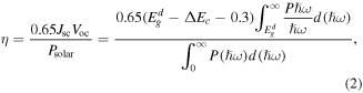
Standard image High-resolution imageThe PCE is another important index to evaluate photocatalyst, and thus the PCE of the BP-MoSe2 vdW heterostructure under strains from −3% to 2% has been evaluated using the formula [64]:
Where  and
and  are the bandgap of the donor and the CBO, respectively. P(
 ω) is the AM 1.5 solar flux at the photon energy
  ω, and
  is the total incident solar power per unit area. The calculated CBM, VBM, bandgaps, bandgaps of the donor, CBO and PCE under strains from −3% to 2% are listed in table 2, where we can see that the PCE of the BP-MoSe2 vdW heterostructure without any strain is 12.7%. Evidently, the PCE is 12.0%, 12.7% and 12.8% under compressive strains of −1%, −2% and −3%, which is not sensitive to the compressive strain. However, the PCE is 16.3% and 20.2% under tensile strains of 1% and 2%, which increases rapidly under the tensile strain. Specially, the PCE is remarkably enhanced to 20.2% under biaxial tensile strain of 2%, which is higher than that of 19.9% in the MoSSe/BlueP vdW heterostructure under a 2% tensile strain [41]. We know from formula (2) that the PCE is inversely proportional to CBO and directly proportional to bandgap of the donor. That is, the value of PCE depends on the competition of CBO and bandgap of the donor. As a result, the PCE can achieve 20.2% under strain of 2% due to the very small CBO value of 0.07 eV. On the other hand, the carrier concentration depends on the temperature and bandgap. The high temperature and narrow bandgap can facilitate the electron excitation, increasing the carrier concentration, and vice versa. Therefore, the BP-MoSe2 vdW heterostructure under strain of 2% has the highest carrier concentration due to its minimum bandgap.
Table 2. Calculated CBM, VBM, bandgaps ( ), bandgaps of the donor (
 ), CBO (ΔEc
) and PCE under strains from −3% to 2%.
), CBO (ΔEc
) and PCE under strains from −3% to 2%.
| Strain (%) | CBM (eV) | VBM (eV) |
 (eV) (eV) |
 (eV) (eV) | ΔEc (eV) | PCE (%) |
|---|---|---|---|---|---|---|
| −3 | 1.43 | −0.20 | 1.63 | 1.99 | 0.36 | 12.8 |
| −2 | 1.49 | −0.24 | 1.72 | 2.04 | 0.32 | 12.7 |
| −1 | 1.51 | −0.23 | 1.75 | 2.08 | 0.34 | 12.0 |
| 0 | 1.50 | −0.23 | 1.73 | 2.04 | 0.31 | 12.7 |
| 1 | 1.41 | −0.23 | 1.64 | 1.83 | 0.20 | 16.3 |
| 2 | 1.33 | −0.22 | 1.56 | 1.63 | 0.07 | 20.2 |
To gain deep insight into the excellent PCE under tensile strains, we further examined the project density of states of the BP-MoSe2 vdW heterostructure under strains of 0%, 1% and 2%. As shown in figure 7, the lowest unoccupied molecular orbital (LUMO) of Mo atom, represents by the light purple line, rapidly decreases as the tensile strain increases from 0% to 1% to 2%. However, the LUMO of Se atom (green line) decreases very slowly with the increase of the tensile strain. Therefore, the CBM of MoSe2 is mainly contributed by 4d of Mo atom. Moreover, the LUMO of Mo atom approaches that of P atom under a 2% tensile strain, which results in the small value of CBO, causing the high PCE value.

Figure 7. Projected density of states (PDOS) of the BP-MoSe2 vdW heterostructure under strains of 0%, 1% and 2%.
Download figure:
Standard image High-resolution imageThe ability to capture Sunlight is another important requisite for an excellent photocatalyst. To examine the light absorption performance of the BP-MoSe2 vdW heterostructure under light, the optical absorption coefficients have been calculated based on the HSE06 functional. Since the tensile strains can enhance the PCE of the BP-MoSe2 vdW heterostructure, the optical absorption coefficients of the BP-MoSe2 vdW heterostructure with 0%, 1% and 2% tensile strains have been considered by the formula [65]:
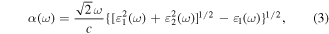
where  and c represent the angular frequency and the speed of light in vacuum, respectively.
  and
and  are the real and imaginary parts of the dielectric function, respectively. As shown in figure 8, the BP-MoSe2 vdW heterostructure without any strains has two notable absorption peaks, the corresponding absorption intensity is ∼4.4 × 105 cm−1 at the wavelength of 415 nm and ∼5.0 × 105 cm−1 at the wavelength of 560 nm. These intensities are even higher than those of other high-efficiency photocatalyst systems [11, 37,41, 63]. Therefore, the BP-MoSe2 vdW heterostructure is efficient light harvesting photocatalysts. In addition, it is found that the first absorption peak has a redshift under the tensile strains of 1% and 2%. Moreover, it should be noted that the tensile strains could broaden the optical absorption of the BP-MoSe2 vdW heterostructure to the near-ultraviolet light spectrum. Specifically, the absorption intensity is ∼5.5 × 105 cm−1 at the wavelength of 358 nm under a 1% strain and ∼4.3 × 105 cm−1 at the wavelength of 379 nm under a 2% strain. Therefore, the tensile strains greatly improve the utilization of Sunlight.

Figure 8. Optical absorption coefficients of the BP-MoSe2 vdW heterostructure under strains of 0%, 1% and 2%.
Download figure:
Standard image High-resolution image3.3. Gibbs free energy profiles for the HER and OER processes
We know from the above analysis that the BP layer is an electron accepter, while the MoSe2 layer is an electron donor in the BP-MoSe2 vdW heterostructure. Once the BP-MoSe2 vdW heterostructure is radiated by sunlight as a photocatalysts, the BP layer will accumulate a large number of electrons, while the MoSe2 layer will accumulate a large number of holes. Therefore, the reduction reaction of  (HER) will occur on the BP layer due to aggregation of electrons, and the oxidation reaction of
  (OER) will occur on the MoSe2 layer due to accumulation of holes. Therefore, the HER performance of BP layer and OER catalytic activity of MoSe2 layer are investigated in the following calculations.
In this work, the changes of Gibbs free energy (ΔG) for the HER and OER processes are calculated using formula as [11]:

where  is the adsorption energy,
  is the difference of zero point vibration energy,
  and
and  are the absolute temperature and entropy change, respectively. Here, for the zero point energy contribution, only the vibrational frequencies of absorbed species are calculated with the BP-MoSe2 heterostructure fixed. Moreover, only vibration entropy contributions are considered for adsorbates, and we take the temperature as 298.15 K. Firstly, the HER process in the acidic environment has been considered. There are two elementary reaction steps for HER:
  and
and  where * represents the active site of the substrate, and
  represents the hydrogen is attached to the substrate. The first step is to describe the adsorption process of hydrogen atom on the substrate, and the second step is to describe the desorption process of hydrogen molecule from the substrate. Here, the standard hydrogen electrode (SHE) approximation is considered, i.e. the
  ion is converted to
  molecule without Gibbs free energy change in the reaction of
  (ΔG = 0).
Figure 9(a) shows the Gibbs free energy profiles with different hydrogen coverages on BP layer in HER process. Evidently, the first step is the limiting step of the HER for all hydrogen coverages from 1H to 4H, and the positive ΔGH* indicates that this process is endothermic and cannot proceed without light illumination or external potential. In addition, the ΔGH* of the third hydrogen is minimum (0.64 eV), whereas the ΔGH* of the fourth hydrogen is maximum (1.34 eV), indicating that the BP-MoSe2 vdW heterostructure is potentially catalyst for the HER at an appropriate hydrogen coverage.

Figure 9. Gibbs free energy (G) profiles in HER process (a) and OER process (b) on the BP-MoSe2 vdW heterostructure at pH = 0. The 1H, 2H, 3H, and 4H represent different H coverage.
Download figure:
Standard image High-resolution image
Then, we turn our attention to the OER process also in the acidic environment. There are four elementary reactions steps in OER process:


and the corresponding ΔG is calculated using


Therefore, the species of 
 and
and  are the intermediates of the elementary reactions.
Figure 9(b) shows the overall Gibbs free energy profiles in the OER process on the MoSe2 layer of the BP-MoSe2 vdW heterostructure. The inserts are the optimal adsorption configurations of OH, O and OOH adsorbed on the MoSe2 layer. Obviously, ΔG of the first three steps is positive while the last step is negative. The third step is rate-limiting with  of 2.57 eV. At the standard potential of water oxidation (U = 1.23 V), the
  of the rate-limiting step will decrease to 1.34 eV, which is comparable to that of the C2N/GaTe type-II heterojunctions [11].
3.4. The carrier mobility of the BP-MoSe2 vdW heterostructure
The carrier mobility has been investigated to further evaluate the photocatalytic performance of the BP-MoSe2 vdW heterostructure. Generally, high carrier mobility could potentially improve the charge utilization for redox reactions before their recombination [10]. On the basis of the Takagi model within the deformation potential approximation [66–68], the acoustic phonon-limited carrier mobility μ can be calculated as

where e,  and
and  are the electron charge, Planck constant and Boltzmann constant, respectively. T is the absolute temperature, here a room temperature of 300 K is used in the calculations. m is the effective mass of carriers along the transport direction, which is defined as
  md
is the average effective mass, which equals
md
is the average effective mass, which equals  (
( is the effective mass perpendicular to the transport direction).
  is the deformation potential constant of the VBM for a hole or the CBM for an electron along the transport directions, which is defined as
  (
( is the band edge shift under lattice deformation,
  is the lattice deformation).
  is the elastic modulus of the 2D heterostructure, which is computed by
 ![${C}_{2{\rm{D}}}={\rm{\Delta }}E/\left[{\left(\tfrac{{\rm{\Delta }}l}{l}\right)}^{2}{S}_{0}\right]$](https://content.cld.iop.org/journals/0957-4484/34/8/085403/revision2/nanoaca548ieqn44.gif) (
( is the energy change of the system under
  and
and  is the area of the BP-MoSe2 vdW heterostructure). It has been demonstrated this model is not only computational efficient but also physically reasonable [69, 70], and has been successfully used in predicting the carrier mobility of 2D semiconductors such as GeAsSe and SnSbTe [63].
Table 3 shows that the carrier mobility displays a fairly pronounced anisotropy, and thus is essential to control the carrier transport directionally to enhance device performance. For example, the mobility of electrons along the x and y directions are 17.01 and 3613.68  respectively, and the mobility of holes along the x and y directions are 523.45 and 235.46
  respectively. These mobilities of carriers are comparable with the theoretically proposed β-AsP monolayer [71] and C2N-based type-II heterojunctions [11]. In addition, the deformation potential constant reflects the strength of electron-phonon coupling, and is determined by the band edge shift under lattice deformation. Further observation finds that the low mobility of electrons along x direction is attributed to its large deformation potential constant (12.86 eV), and thus significantly reduces the electron mobility.
Table 3. The effective mass of carriers (in m0), deformation potential constants (in eV), elastic modulus (in  ), and mobility of carriers (in
  ) along x and y directions.
| Material | Carrier |

|

|

|

|

|

|

|

|
|---|---|---|---|---|---|---|---|---|---|
| BP-MoSe2 | e | 1.42 | 0.78 | 12.86 | 1.17 | 196.47 | 189.85 | 17.01 | 3613.68 |
| h | 0.57 | 0.83 | 4.52 | 5.49 | 196.47 | 189.85 | 523.45 | 235.46 |
4. Conclusions
To summarize, we have theoretically shown that the stability, geometric and electronic structures, biaxial strain effects, band edge positions, PCE and optical absorption, Gibbs free energy for HER and OER, as well as the carriers mobility of the BP-MoSe2 vdW heterostructure via first-principles calculations. The main findings are summarized in follows:
- (1)The BP-MoSe2 vdW heterostructure is energetically stable with a negative formation energy of −0.21 eV and has thermodynamic stability evaluated from AIMD simulations. In addition, the interfacial distance of the BP-MoSe2 vdW heterostructure is 3.17 Å, and thus the BP layer interacts with the MoSe2 layer through week vdW force.
- (2)The BP-MoSe2 vdW heterostructure is type-II band alignment semiconductor with indirect bandgap of 1.73 eV, the VBM and CBM are from the MoSe2 and BP monolayer, respectively. This allows the heterostructure to effectively separate the photogenerated electron–hole pairs.
- (3)The BP-MoSe2 vdW heterostructure under biaxial strains from −3% to 2% still maintains type-II band characteristics. Moreover, the band edge positions straddle the redox potentials of water, which indicates that the BP-MoSe2 vdW heterostructure under strains of −3% to 2% is promising candidate for photocatalytic water splitting without an external bias voltage in acidic environments.
- (4)The BP-MoSe2 vdW heterostructure possesses significantly high PCE, e.g. ∼13% without strain and ∼20% under a 2% tensile strain. In addition, the heterostructure also has strong optical absorption in the visible light and near-ultraviolet region. Specifically, the absorption intensity is ∼4.4 to 5.0 × 105 cm−1 without strain and ∼4.3 to 5.5 × 105 cm−1 under 1% and 2% tensile strains. Therefore, the BP-MoSe2 vdW heterostructure is an efficient light harvesting photocatalysts, and the tensile strains greatly improve the PCE and optical absorption.
- (5)The ΔGH* is 0.64 eV for 3H coverage at U = 0 V and 0.11 eV for 4H coverage at U = 1.23 V, indicating that the BP-MoSe2 vdW heterostructure is a potentially catalyst for the HER at an appropriate hydrogen coverage. Moreover, the BP-MoSe2 heterostructure has a good OER catalytic performance.
- (6)The calculations of carrier mobility indicate that the BP-MoSe2 vdW heterostructure has higher carrier mobility compared to other proposed high-efficiency photocatalyst, which indicates that the transfer of charge carriers to the reactive sites is easier, reducing the probability of recombination of photogenerated electron–hole pairs.
In short, the results of our calculations evidenced that the BP-MoSe2 vdW heterostructure is very promising photocatalysts for water splitting with the moderate band gaps, suitable band edge positions, excellent PCE, strong optical absorption, good catalytic performance for HER and OER, and high carrier mobility based on accurate HSE06 calculations.
Acknowledgments
The authors thank the National Natural Science Foundation of China (Grant Nos. 12164020) and the Natural Science Foundation of Jiangxi Province (Grant No. 20202BAB201012) for financial support of the current work. We gratefully acknowledge Hefei Advanced Computing Center for computational support.
Data availability statement
The data that support the findings of this study are available upon reasonable request from the authors.