Southbridge (computing): Difference between revisions
Magioladitis (talk | contribs) m →Functionality: clean up using AWB (8514) |
Platform Controller Hub |
||
| Line 5: | Line 5: | ||
The southbridge can usually be distinguished from the northbridge by not being directly connected to the [[Central processing unit|CPU]]. Rather, the northbridge ties the southbridge to the CPU. Through the use of controller integrated channel circuitry, the northbridge can directly link signals from the I/O units to the CPU for data control and access. |
The southbridge can usually be distinguished from the northbridge by not being directly connected to the [[Central processing unit|CPU]]. Rather, the northbridge ties the southbridge to the CPU. Through the use of controller integrated channel circuitry, the northbridge can directly link signals from the I/O units to the CPU for data control and access. |
||
Due to the push for [[System on a chip|System-on-a-chip]] (SoC) processors, modern devices increasingly have the northbridge integrated into the CPU [[Die (integrated circuit)|die]] itself; examples are [[Intel]]'s [[Sandy Bridge]] and [[AMD]]'s [[AMD Fusion|Fusion]] processors (both released in 2011). In such cases the southbridge is being directly connected to the CPU. Intel's [[Haswell (microarchitecture)|Haswell]], expected to be available in 2013, is expected to feature the southbridge on the same package as the CPU for the [[Ultrabook]] platform.{{Citation needed|date=April 2012}} |
Due to the push for [[System on a chip|System-on-a-chip]] (SoC) processors, modern devices increasingly have the northbridge integrated into the CPU [[Die (integrated circuit)|die]] itself; examples are [[Intel]]'s [[Sandy Bridge]] and [[AMD]]'s [[AMD Fusion|Fusion]] processors (both released in 2011). In such cases the southbridge is being directly connected to the CPU. Intel's [[Haswell (microarchitecture)|Haswell]], expected to be available in 2013, is expected to feature the southbridge ([[Platform Controller Hub]]) on the same package as the CPU for the [[Ultrabook]] platform.{{Citation needed|date=April 2012}} |
||
==Overview== |
==Overview== |
||
Revision as of 08:04, 18 November 2012


The southbridge is one of the two chips in the core logic chipset on a personal computer (PC) motherboard, the other being the northbridge. The southbridge typically implements the slower capabilities of the motherboard in a northbridge/southbridge chipset computer architecture. In Intel chipset systems, the southbridge is named Input/Output Controller Hub (ICH). AMD, beginning with its Fusion APUs, has given the label FCH, or Fusion Controller Hub, to its southbridge.
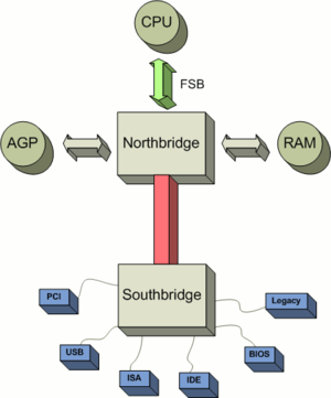
The southbridge can usually be distinguished from the northbridge by not being directly connected to the CPU. Rather, the northbridge ties the southbridge to the CPU. Through the use of controller integrated channel circuitry, the northbridge can directly link signals from the I/O units to the CPU for data control and access.
Due to the push for System-on-a-chip (SoC) processors, modern devices increasingly have the northbridge integrated into the CPU die itself; examples are Intel's Sandy Bridge and AMD's Fusion processors (both released in 2011). In such cases the southbridge is being directly connected to the CPU. Intel's Haswell, expected to be available in 2013, is expected to feature the southbridge (Platform Controller Hub) on the same package as the CPU for the Ultrabook platform.[citation needed]
Übersicht
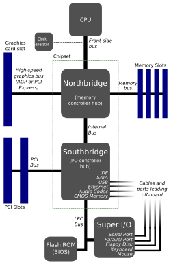
A southbridge chipset handles all of a computer's I/O functions, such as USB, audio, serial, the system BIOS, the ISA bus, the interrupt controller and the IDE channels.[1] Different combinations of Southbridge and Northbridge chips are possible,[2] but these two kinds of chip must be designed to work together;[3][4] there is no industry-wide standard for interoperability between different core logic chipset designs. Traditionally, the interface between a northbridge and southbridge was the PCI bus. The main bridging interfaces used now are DMI (Intel) and UMI (AMD).
Etymology
The name is derived from drawing the architecture in the fashion of a map and was first described as such with the introduction of the PCI Local Bus Architecture in 1991. At Intel, the authors of the PCI specification viewed the PCI local bus as being at the very centre of the PC platform architecture (i.e., at the Equator).
The northbridge extends to the north of the PCI bus backbone in support of CPU, Memory/Cache, and other performance-critical capabilities. Likewise the southbridge extends to the south of the PCI bus backbone and bridges to less performance-critical I/O capabilities such as the disk interface, audio, etc.
The CPU is located at the top of the map at due north. The CPU is connected to the chipset via a fast bridge (the northbridge) located north of other system devices as drawn. The northbridge is connected to the rest of the chipset via a slow bridge (the southbridge) located south of other system devices as drawn.
Although the current PC platform architecture has replaced the PCI bus backbone with faster I/O backbones, the bridge naming convention remains.
Functionality

The functionality found in a contemporary southbridge includes:[4]
- PCI bus. The PCI bus support includes the traditional PCI specification, but may also include support for PCI-X and PCI Express.
- ISA bus or LPC Bridge. Though the ISA support is rarely utilized, it has interestingly managed to remain an integrated part of the modern southbridge. The LPC Bridge provides a data and control path to the Super I/O (the normal attachment for the keyboard, mouse, parallel port, serial port, IR port, and floppy controller) and FWH (firmware hub which provides access to BIOS flash storage).
- SPI bus. The SPI bus is a simple serial bus mostly used for firmware (e.g., BIOS) flash storage access.
- SMBus. The SMBus is used to communicate with other devices on the motherboard (e.g., system temperature sensors, fan controllers).
- DMA controller. The DMA controller allows ISA or LPC devices direct access to main memory without needing help from the CPU.
- Interrupt controllers such as 8259A and/or I/O APIC. The interrupt controller provides a mechanism for attached devices to get attention from the CPU.
- Mass storage controllers such as PATA and/or SATA. This typically allows direct attachment of system hard drives.
- Real-time clock. The real time clock provides a persistent time account.
- Power management (APM and ACPI). The APM or ACPI functions provide methods and signaling to allow the computer to sleep or shut down to save power.
- Nonvolatile BIOS memory. The system CMOS, assisted by battery supplemental power, creates a limited non-volatile storage area for system configuration data.
- AC'97 or Intel High Definition Audio sound interface.
- Out-of-band management controller such as a BMC or HECI.
Optionally, a southbridge also includes support for Ethernet, RAID, USB, audio codec, and FireWire. Where support is provided for non-USB keyboard, mouse, and serial ports, a machine normally does so through a device referred to as a Super I/O; still more rarely, a southbridge may directly support the keyboard, mouse, and serial ports.
See also
References
External links
- "InformIT: Motherboards & Core-Logic Chipsets: The Deep Stuff > What the North Bridge and South Bridge Do". Retrieved November 18, 2010.
