
Photoresist
A photoresist is a light-sensitive material used in several processes, such as photolithography and photoengraving, to form a patterned coating on a surface, which is crucial in the whole electronic industry.[1]

Definitions
Positive Photoresist

A positive resist is a type of photoresist in which the portion of the photoresist that is exposed to light becomes soluble to the photoresist developer. The unexposed portion of the photoresist remains insoluble to the photoresist developer.
Negative Photoresist
A negative photoresist is a type of photoresist in which the portion of the photoresist that is exposed to light becomes insoluble to the photoresist developer. The unexposed portion of the photoresist is dissolved by the photoresist developer.

Differences between Positive and Negative Resist[3]
| Characteristic | Positive | Negative |
| Adhesion to Silicon | Fair | Excellent |
| Relative Cost | More expensive | Less expensive |
| Developer Base | Aqueous | Organic |
| Solubility in the developer | Exposed region is soluble | Exposed region is insoluble |
| Minimum Feature | 0.5 µm | 2 µm |
| Step Coverage | Better | Lower |
| Wet Chemical Resistance | Fair | Excellent |
Note: This table is based on generalizations which are generally accepted in the Microelectromechanical systems(MEMS) Fabrication industry.
Types of Photoresist
Based on the chemical structure of photoresists, they can be classified into three types:
Photopolymeric, photodecomposing, photocrosslinking photoresist.
Photopolymeric Photoresist
Photopolymeric photoresist is a type of photoresist, usually allyl monomer, which could generate free radical when exposed to light, then initiates the photopolymerization of monomer to produce a polymer. Photopolymeric photoresists are usually used for negative photoresist, e.g. methyl methacrylate.

Photodecomposable Photoresist
Photodecomposing photoresist is a type of photoresist that generates hydrophilic productunder light. Photodecomposing photoresists are usually used for positive photoresist. A typical example is azide quinone, e.g. diazonaphthaquinone (DQ).

Photocrosslinking Photoresist
Photocrosslinking photoresist is a type of photoresist, which could crosslink chain by chain when exposed to light, to generate an insoluble network. Photocrosslinking photoresist are usually used for negative photoresist.
(1) SU-8

(2) Off-Stoichiometry Thiol-Enes (OSTE) polymers[4]
Self-assembled Monolayer (SAM) Photoresist
For SAM photoresist, first an SAM is formed on the substrate by self-assembly. Then, this surface covered by SAM is irradiated through a mask, similar to other photoresist, which
generates a photo-patterned sample in the irradiated areas. And finally developer is used to remove the designed part (could be used as both positive or negative photoresist).[5]
Light Sources
Adsortption at UV and shorter wavelengths
In lithography, decreasing the wavelength of light source is the most efficient way to achieve higher resolution.[6] Photoresists are most commonly used at wavelengths in the ultraviolet spectrum or shorter (<400 nm). For example, diazonaphthoquinone (DNQ) absorbs strongly from approximately 300 nm to 450 nm. The absorption bands can be assigned to n-π* (S0–S1) and π-π* (S1–S2) transitions in the DNQ molecule.[7] In the deep ultraviolet (DUV) spectrum, the π-π* electronic transition in benzene[8] or carbon double-bond chromophores appears at around 200 nm.[9] Due to the appearance of more possible absorption transitions involving larger energy differences, the absorption tends to increase with shorter wavelength, or larger photon energy. Photons with energies exceeding the ionization potential of the photoresist (can be as low as 5 eV in condensed solutions)[10] can also release electrons which are capable of additional exposure of the photoresist. From about 5 eV to about 20 eV, photoionization of outer "valence band" electrons is the main absorption mechanism.[11] Above 20 eV, inner electron ionization and Auger transitions become more important. Photon absorption begins to decrease as the X-ray region is approached, as fewer Auger transitions between deep atomic levels are allowed for the higher photon energy. The absorbed energy can drive further reactions and ultimately dissipates as heat. This is associated with the outgassing and contamination from the photoresist.
Electron-beam exposure
Photoresists can also be exposed by electron beams, producing the same results as exposure by light. The main difference is that while photons are absorbed, depositing all their energy at once, electrons deposit their energy gradually, and scatter within the photoresist during this process. As with high-energy wavelengths, many transitions are excited by electron beams, and heating and outgassing are still a concern. The dissociation energy for a C-C bond is 3.6 eV. Secondary electrons generated by primary ionizing radiation have energies sufficient to dissociate this bond, causing scission. In addition, the low-energy electrons have a longer photoresist interaction time due to their lower speed; essentially the electron has to be at rest with respect to the molecule in order to react most strongly via dissociative electron attachment, where the electron comes to rest at the molecule, depositing all its kinetic energy.[12] The resulting scission breaks the original polymer into segments of lower molecular weight, which are more readily dissolved in a solvent, or else releases other chemical species (acids) which catalyze further scission reactions (see the discussion on chemically amplified resists below).It is not common to select photoresists for electron-beam exposure. Electron beam lithography usually relies on resists dedicated specifically to electron-beam exposure.
Parameters for photoresist[13]
Resolution is defined as the ability to differ the neighboring features on the substrate. Critical dimension (CD) is a main measure of resolution.
The smaller the critical dimension is, the higher resolution would be.
Contrast is defined as the gradience from exposure portion to unexposure portion. The Higher contrast is, the more obvious difference between exposure portion and unexposure portion would be.
Sensitivity
Sensitivity is defined as the minimum energy that is required to generate a well-defined feature in the photoresist on the substrate. Unit: mJ/cm2.
The sensitivity of a photoresist is important when using deep ultraviolet (DUV) or extra-deep ultraviolet (EUV).
Viscosity is defined as a quantity of the photoresist, expressing the magnitude of internal friction. Specific gravity (SG) is a measure of viscosity of a photoresist. Unit: poise or cps, 1 cps = 0.01 poise.
When it is needed to produce a thicker layer, the photoresist with higher viscosity will be preferred.
Adherence is defined as the adhesive strength between photoresist and substrate. The inefficient adherence of photoresist to substrate may lead to the deformation of the generated features.
Anti-etching
Anti-etching is defined as the ability of a photoresist to resist the high temperature, different pH environment or the ion bombardment in the possess of post-modification.
Surface tension is defined as the tension that induced by a liquid tended to minimize its surface area, which is caused by the attraction of the particles in the surface layer.
In order to better cover the surface of substrate, photoresists are required to possess relatively low surface tension.
Positive Photoresist
DNQ-Novolac photoresist
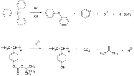
One very common positive photoresist used with the I, G and H-lines from a mercury-vapor lamp is based on a mixture of diazonaphthoquinone (DNQ) and novolac resin (a phenol formaldehyde resin). DNQ inhibits the dissolution of the novolac resin, but upon exposure to light, the dissolution rate increases even beyond that of pure novolac. The mechanism by which unexposed DNQ inhibits novolac dissolution is not well understood, but is believed to be related to hydrogen bonding (or more exactly diazocoupling in the unexposed region). DNQ-novolac resists are developed by dissolution in a basic solution (usually 0.26N tetramethylammonium hydroxide (TMAH) in water).
Chemical structure and mechanism of DNQ-Novolac photoresist are shown.
Negative Photoresist
Epoxy-based polymer
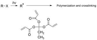
One very common negative photoresist is based on epoxy-based polymer. The common product name is SU-8 photoresist, and it was originally invented by IBM, but is now sold by Microchem and Gersteltec. One unique property of SU-8 is that it is very difficult to strip. As such, it is often used in applications where a permanent resist pattern (one that is not strippable, and can even be used in harsh temperature and pressure environments) is needed for a device.[14] Mechanism of epoxy-based polymer is shown in 1.2.3 SU-8.
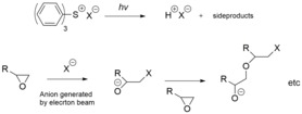
Off-Stoichiometry Thiol-Enes(OSTE) polymer
In 2016, OSTE Polymers were shown to possess a unique photolitography mechanism, based on diffusion-induced monomer depletion, which enables high photostructuring accuracy. The OSTE polymer material was originally invented at the KTH Royal Institute of Technology, but is now sold by Mercene Labs. Whereas the material has properties similar to those of SU8, OSTE has the specific advantage that it contains reactive surface molecules, which make this material attractive for microfluidic or biomedical applications.[15]
Chemical structure and mechanism of OSTE polymer as negative photoresist are shown.
Applications
Microcontact printing was described by Whitesides Group in 1993. Generally, in this techniques, an elastomeric stamp is used to generate two-dimensional patterns, through printing the “ink” molecules onto the surface of a solid substrate.


Step 1 for microcontact printing. A scheme for the creation of a polydimethylsiloxane(PDMS) master stamp. Step 2 for microcontact printing A scheme of the inking and contact process of microprinting lithography.
Fabrication of printed circuit boards (PCB)
Printed circuit boards is one of the most important applications of photoresist. The general is that by applying photoresist, exposing image to ultraviolet rays, and then etching using iron chloride, cupric chloride or an alkaline ammonia etching solution to remove the copper-clad substrate.[17]
Well known photoresist materials used in the PCB industry:[18]
FR-4 (woven glass and epoxy) - most common material today
FR-5 (woven glass and epoxy)
FR-6 (cotton paper and epoxy)
G-10 (woven glass and epoxy)
CEM-1 (cotton paper and epoxy)
CEM-5 (woven glass and polyester)

A PCB sample
Patterning and etching of substrates
This includes specialty photonics materials, Micro-Electro-Mechanical Systems(MEMS), glass printed circuit boards, and other micropatterning tasks. Photoresist tends not to be etched by solutions with a pH greater than 3.[19]

MEMS microcantilever resonating in an SEM
This application, mainly applied to silicon wafers/silicon integrated circuits is the most developed of the technologies and the most specialized in the field.[20]

A 12-inch silicon wafer
References
- ^ Eric, Anslyn; Dougherty, Dennis. Modern physical organic chemistry. University Science Books.
- ^ Ito, H.; Willson, C. G.; Frechet, J. H. J. (1982-09-01). "New UV Resists with Negative or Positive Tone". 1982 Symposium on VLSI Technology. Digest of Technical Papers: 86–87.
- ^ Madou, Marc. Fundamentals of Microfabrication. CRC Press. ISBN 0-8493-0826-7.
- ^ "Dry adhesive bonding of nanoporous inorganic membranes to microfluidic devices using the OSTE(+) dual-cure polymer". Journal of Micromechanics and Microengineering.
- ^ Huang, Jingyu; Dahlgren, David A.; Hemminger, John C. (1994-03-01). "Photopatterning of Self-Assembled Alkanethiolate Monolayers on Gold: A Simple Monolayer Photoresist Utilizing Aqueous Chemistry". Langmuir. 10 (3): 626–628. doi:10.1021/la00015a005. ISSN 0743-7463.
- ^ Bratton, Daniel; Yang, Da; Dai, Junyan; Ober, Christopher K. (2006-02-01). "Recent progress in high resolution lithography". Polymers for Advanced Technologies. 17 (2): 94–103. doi:10.1002/pat.662. ISSN 1099-1581.
- ^ [che.gatech.edu "DNQ-novolac photoresists"].
{{cite web}}: Check|url=value (help); Cite has empty unknown parameter:|dead-url=(help) - ^ Ishii, Hiroyuki; Usui, Shinji; Douki, Katsuji; Kajita, Toru; Chawanya, Hitoshi; Shimokawa, Tsutomu (2000-01-01). "Design and lithographic performances of 193-specific photoacid generators". 3999: 1120–1127. doi:10.1117/12.388276.
{{cite journal}}: Cite journal requires|journal=(help) - ^ [Cem.msu.edu "UV-Visible Spectroscopy"].
{{cite web}}: Check|url=value (help); Cite has empty unknown parameter:|dead-url=(help) - ^ Belbruno, Joseph. "Multiphoton-induced chemistry of phenol in hexane at 266 nm". Chemical Physics Letters.
- ^ "Photoelectric Emission from Dust Grains Exposed to Extreme Ultraviolet and X-Ray Radiation". The Astrophysical Journal.
- ^ "IR photon enhanced dissociative electron attachment to SF6: Dependence on photon, vibrational, and electron energ". Chemical Physics.
- ^ Greener, Jesse; Li, Wei; Ren, Judy; Voicu, Dan; Pakharenko, Viktoriya; Tang, Tian; Kumacheva, Eugenia (2010-02-02). "Rapid, cost-efficient fabrication of microfluidic reactors in thermoplastic polymers by combining photolithography and hot embossing". Lab Chip. 10 (4): 522–524. doi:10.1039/b918834g. ISSN 1473-0189.
- ^ DeForest, William S (1975). Photoresist: materials and processes. McGraw-Hill Companies.
- ^ Greener, Jesse; Li, Wei; Ren, Judy; Voicu, Dan; Pakharenko, Viktoriya; Tang, Tian; Kumacheva, Eugenia (2010-02-02). "Rapid, cost-efficient fabrication of microfluidic reactors in thermoplastic polymers by combining photolithography and hot embossing". Lab Chip. 10 (4): 522–524. doi:10.1039/b918834g. ISSN 1473-0189.
- ^ "Self-assembled Monolayer Films: Microcontact Printing" (PDF).
{{cite web}}: Cite has empty unknown parameter:|dead-url=(help) - ^ Montrose, Mark I (1999). The Electronic Packaging Handbook. CRC Press.
- ^ Jawitz, Martin W (1997). Printed circuit board materials handbook. McGraw Hill Professional.
- ^ Novak, R.E (2000). Cleaning Technology in Semiconductor Device Manufacturing. Electrochemical Society Inc. ISBN 1566772591.
- ^ Silicon photonics. Springer Science & Business Media. 2004.